Influence of electron and ion beam irradiation on solid electrolytes during imaging and sample fabrication
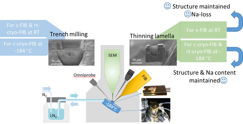
Although all solid-state batteries have promising future in the battery industry due to their high energy density and excellent safe behavior, they still suffer from interfacial problems, to the solid electrolyte (SE), which is delaying their commercialization progress. Electron microscopy coupled with spectroscopy is a powerful tool for investigating these mechanisms from an atomic to microscopic length scale. However, a reliable characterization of these interfaces involving SEs using electron microscopy presents challenges as they can be already damaged by electron and ion beam irradiation during sample preparation. To overcome these limitations, a cryoFIB workflow has been established for SEM imaging and TEM sample preparation (Figure 1).
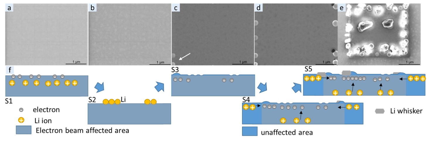
In this work, different SEs have been studied in dual-beam SEM/FIB (FEI Strata & Zeiss Auriga). Figure 2 shows SEM images of lithium phosphorus oxynitride (LiPON) at different electron doses but the same acceleration voltage of 2kV. An electric field can be generated due to the blocked electrons with imaging to drive the Li+ ions movement towards to the sample surface and reduction to form Li particles.
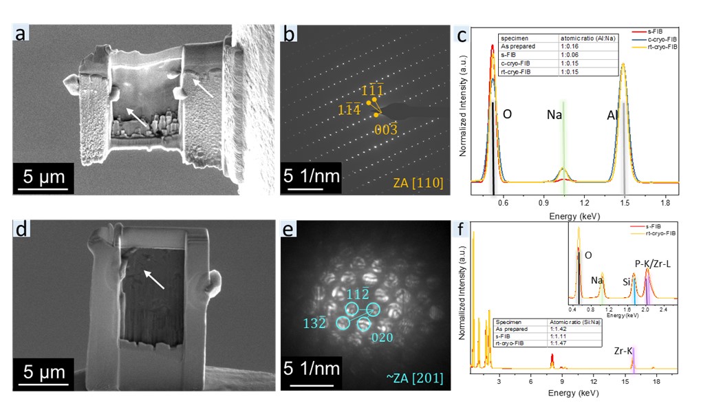
A similar phenomenon was also found during TEM sample preparation using FIB when SEs were polished as shown in Figure 3. As indicated by the white arrows, Na particles formed at the viewing surface. Electron diffraction (Figure 3b, e) shows no changes in the crystal structure. However, compositional studies using EDS reveal a loss of Na (Figure 3c, f) and TEM analysis further shows crack formation introduced during room temperature FIB preparation.
In order to reduce morphological changes and ion migration during imaging, it is necessary to coat the SE with a conductive layer to reduce charging and thus charging driven ion migration. Even better works the application of cryogenic imaging and preparation conditions, which prevents ion migration and thus structural and compositional changes efficiently.
 |
This work is founded by the German Research Foundation (DFG) under Project ID 390874152 (POLiS Cluster of Excellence) and published in Microscopy (Oxford). Details can be found in https://doi.org/10.1093/jmicro/dfac064. |
|
Figure 1. Dual-beam focus ion beam microscopy equipped with cryogenic stage. |
Figure 2. SEM imaging at 2 kV of a LiPON thin film with increasing dose and corresponding simplified model of the processes in the SEM: a. initial thin film morphology; b. after 22 e/nm2; c. after 433 e/nm2; d. after 995 e/nm2; e. de-magnified SEM image after 3500 e/nm2; f. simplified model of the structural changes observed with increasing dose in the SEM. |
|
Figure 3. a – c. Na-β’’-alumina TEM lamella fabricated by standard FIB at room temperature (RT): a. SEM image during thinning process in FIB; b. selected area electron diffraction; c. EDS of its lamella fabricated at different condition; d – e. Na3.4Si2.4Zr2P0.6O12 (NaSICON) TEM lamella fabricated by standard FIB at room temperature (RT): d. SEM image during thinning process in FIB; e. selected area electron diffraction; f. EDS of its lamella fabricated at different condition; |