Plasticity in Nanocrystalline Metals
Whereas the plastic deformation in coarse-grained metals is governed by their dislocation activity, dislocations are increasingly limited with decreasing grain sizes in nanocrystalline metals. Instead grain boundary dominated processes have been postulated to play an increasing role. A variety of different deformation mechanisms ranging e.g. from grain boundary sliding and grain rotation to the formation of local shear planes and ultimately grain growth are discussed in literature. As part of the DFG Forschergruppe 714 "Plasticity in Nanocrystalline Metals", we are contributing to further elucidate on the deformation mechanisms active in nanocrystalline metals using a variety of ex situ and in situ TEM techniques to directly image their structural and structural changes during the deformation process.
1. Direct imaging of the atomic structure of a triple line in ncPd and it's strain field
In collaboration with Julia Ivanisenko's group at KIT and Gerhard Wilde's group at the University of Munster, we have used aberration corrected HRTEM imaging of HPT deformed ncPd to image the atomic structure of a grain exhibiting a complex network of ∑3 and ∑9 boundaries. In particular, we could image the atomic structure of a triple line formed at the intersection of two coherent twin-boundaries and a ∑9 boundary. The strain field around the triple line measured by geometric phase analysis (GPA) is similar to that of a dislocation in good agreement with molecular dynamics simulations of that triple line.
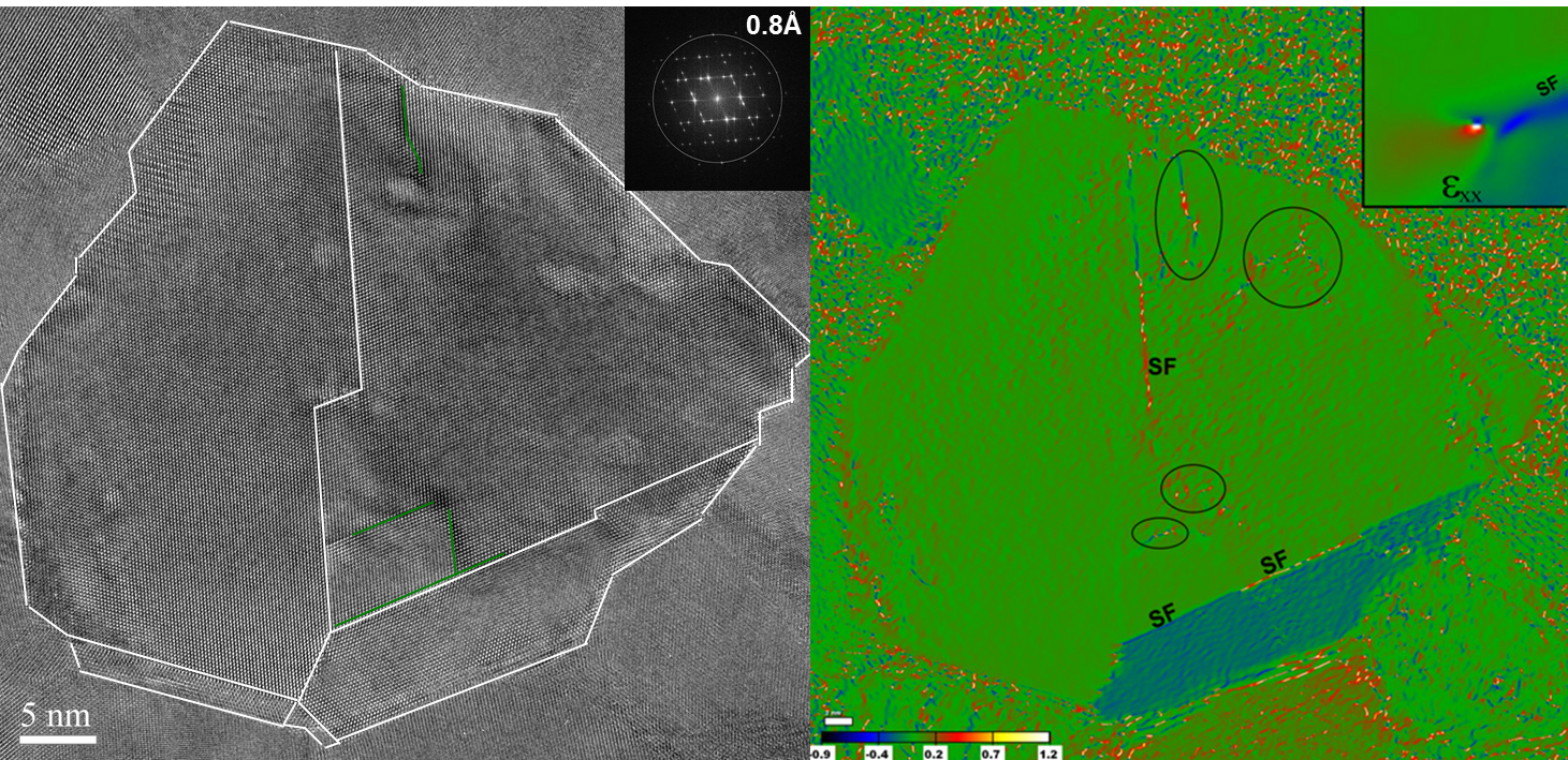
Fig. 1.1: HRTEM image and exx component of the strain map determined by GPA.
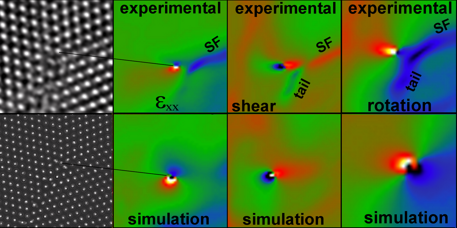
Fig. 1.2: HRTEM image of the triple line and the corresponding strain components - experimental data and MD simulation.
Furthermore, the two different directions of the rigid body rotation observed along the ∑9 boundary in the GPA analysis suggest that two disclinations are present in this grain, at the triple line and a neighboring quadruple line. The two disclinations cannot move independently from each other without introducing long range strain in the sample, which could be an explanation for the higher thermal stability of the HPT deformed ncPd compared to the as prepared ncPd.

Fig. 1.3: Rigid body rotation determined by GPA analysis along the ∑9 boundary.
Details of this work have been published at
- Strain mapping of a triple junction in nanocrystalline Pd, H. Rösner, C. Kübel, J. Ivanisenko, L. Kurmanaeva, S. Divinski, M. Peterlechner, G. Wilde “Strain mapping of a triple junction in nanocrystalline Pd” Acta Mat., 2011, 59, 7380-7387, DOI: 10.1016/j.actamat.2011.08.020.
2. Direct imaging of the structural changes in nanocrystalline Au by in situ straining combined with ACOM-STEM
In order to directly follow the deformation processes in nanocrystalline metals, we have developed the combination of quantitative ACOM-STEM with in situ straining to image changes in the grain structure during straining. A thin nanocrystalline Au film has been deposited on a Push-to-Pull (PTP) device and strained using a Hysitron PI95 indenter in the TEM while measuring the mechanical load. During holding segments of the straining process, the NanoMegas ASTAR system was used to acquire automated crystal orientation (ACOM) maps.
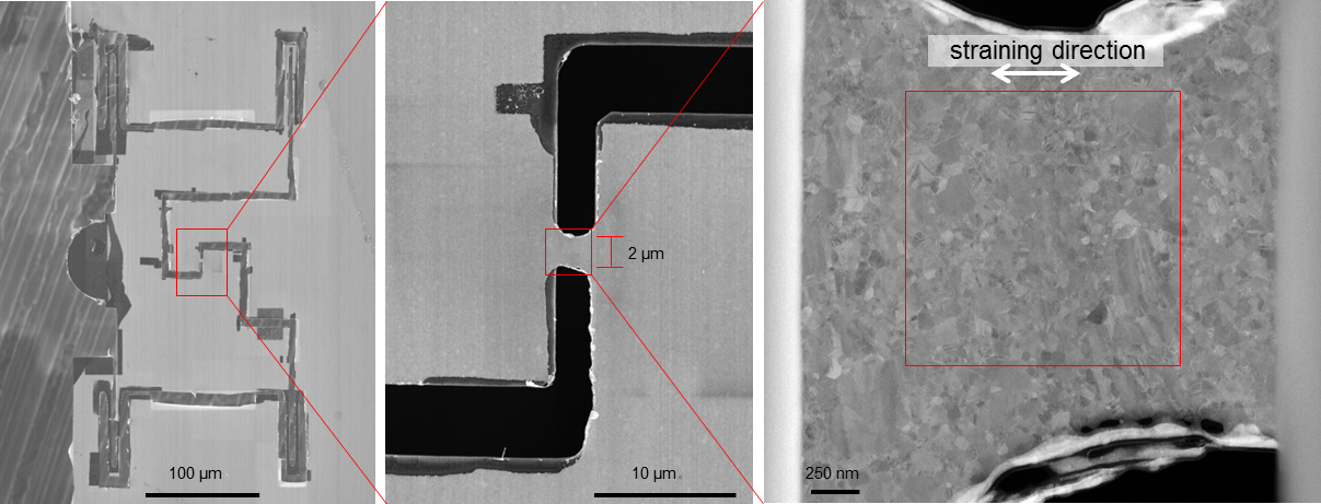
Fig. 2.1: PTP device with a roughly 2 x 2 x 0.05 µm ncAu film for in situ straining the in the TEM
The orientation maps were processed for noise reduction and all reliably indexed grains analyzed using an extended version of Mtex for quantification. The local analysis of the grain structure reveals that grain growth (Fig. 2.2), grain rotation (Fig. 2.3) and (de)twining (Fig. 2.4) are all active during the deformation and can already be observed early in the micro-plastic deformation regime.

Fig. 2.2: Anomalous grain growth during straining of a thin ncAu film.
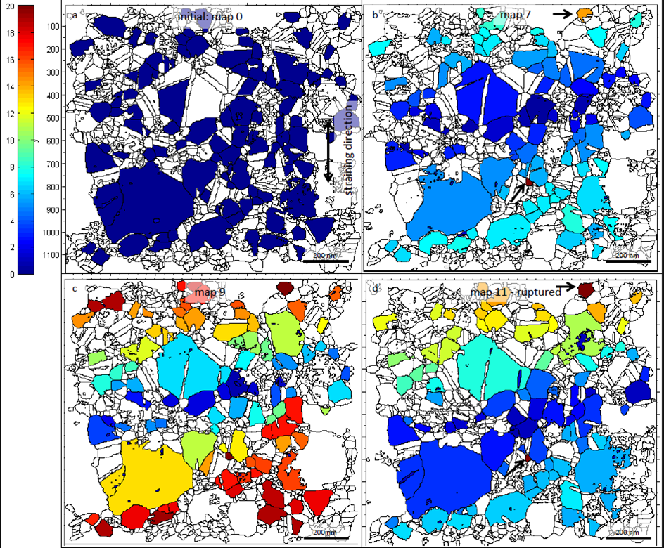
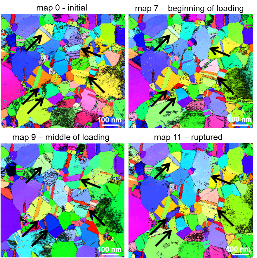
Fig. 2.3: Grain rotation observed during straining of a thin ncAu film.
Fig. 2.4: Simultaneous twining and detwining observed during straining of a thin ncAu film.
The plastic deformation induced during straining is partially reversible, leading e.g. to twin boundaries appearing and disappearing at almost the same location during the different stages of straining and after relaxation. This behavior is presumably due to a Bauschinger type effect as the different grains locally react very differently to the strain, leading to high stress accumulation at their interfaces, which apparently compensates for part of the plastic deformation during relaxation of the sample.
Details of this work have been published at
-
A. Kobler, C. Kübel „Challenges in Quantitative Crystallographic Characterization of 3D thin films by ACOM-TEM” Ultramicroscopy, 2017, 173, 84-94; DOI: 10.1016/j.ultramic.2016.07.007.
- A. Kobler, C. Brandel, H. Hahn, C. Kübel, "In situ observation of deformation processes in nanocrystalline face-centered cubic metals", Beilstein Journal of Nanotechnology, 2016, 7, 572–580; DOI: 10.3762/bjnano.7.50.
-
A. Kobler, A. Kashiwar, H. Hahn, C. Kübel „Combination of in-situ straining and ACOM TEM: a novel method for analysis of plastic deformation of nanocrystalline metals” Ultramicroscopy, 2013, 128, 68-81; DOI: 10.1016/j.ultramic.2012.12.019.
and are available as Bruker webinar on "In-situ mechanics in the TEM".
This project is third-party funded by the DFG as part of the DFG Forschergruppe 714
3. Bauschinger Effect in Nanocrystalline Thin Films
In order further understand the processes in the pseudo-elastic or microplastic regime during the deformation of the nanocrystalline thin films and in particular to confirm and further study the strong Bauschinger effect observed above, recent work has been focused on getting high-quality mechanical data in combination with BF/DF-TEM imaging to better understand dislocation processes during the deformation.
The mechanical data obtained for a nanocrystalline Palladium thin film strained increasingly using the Hysitron Picoindenter reveals the characteristic non-linear unloading curve, where the deviation from the elastic unloading is typically associated with a Bauschinger effect (Fig. 3.1). The corresponding BF-TEM image series (not shown) indicate noticeable local orientation changes as confirmed before by ACOM and a significant dislocation activity already during the very early stages of deformation as well as throughout the whole unloading of the thin film confirming that local stress build up is driving a (partially) reversible dislocation motion during unloading.

Details of this work have been presented as part of the Bruker webinar on "In-situ mechanics in the TEM".

This project is partially third-party funded by the DAAD PhD scholarship of Ankush Kashiwar.
4. Microstructural evolution in multi-layered thin films under tribological loading
Nano-scaled multilayer films are well known for their high strength, hardness and wear resistance. Understanding the deformation mechanisms and processes in these multilayers is essential to optimize their tribological properties. Factors such as layer spacing, modulus mismatch, grain size, coherency and the crystallography of the interfaces govern the mechanical properties of these nanolayered composites. In current research, we try to correlate these parameters with the observed deformation structure in order to understand the tribological deformation processes in collaboration with Dr. Ruth Schwaiger’s group at KIT.
Using automated crystal orientation mapping (ACOM) in STEM, we found that partially coherent Au-Cu multilayers with an initially high twin density deform by grain growth and detwinning initially with the layer structure. With increasing sliding cycles, a vortex like co-deformation was observed, ultimately leading to a mechanical intermixing of the Au and Cu layers (Fig. 4.1). In case of incoherent Cu-Cr multilayers, grain growth/elongation perpendicular to the loading direction was observed in all Cu layers, whereas no noticeable change in grain size was detected in the hard Cr layers (Fig. 4.2). No intermixing of the Cu and the Cr layer has been observed initially, but at high sliding cycles Cu is penetrating between Cr grains ultimately leading to a fragmentation of the Cr layers.
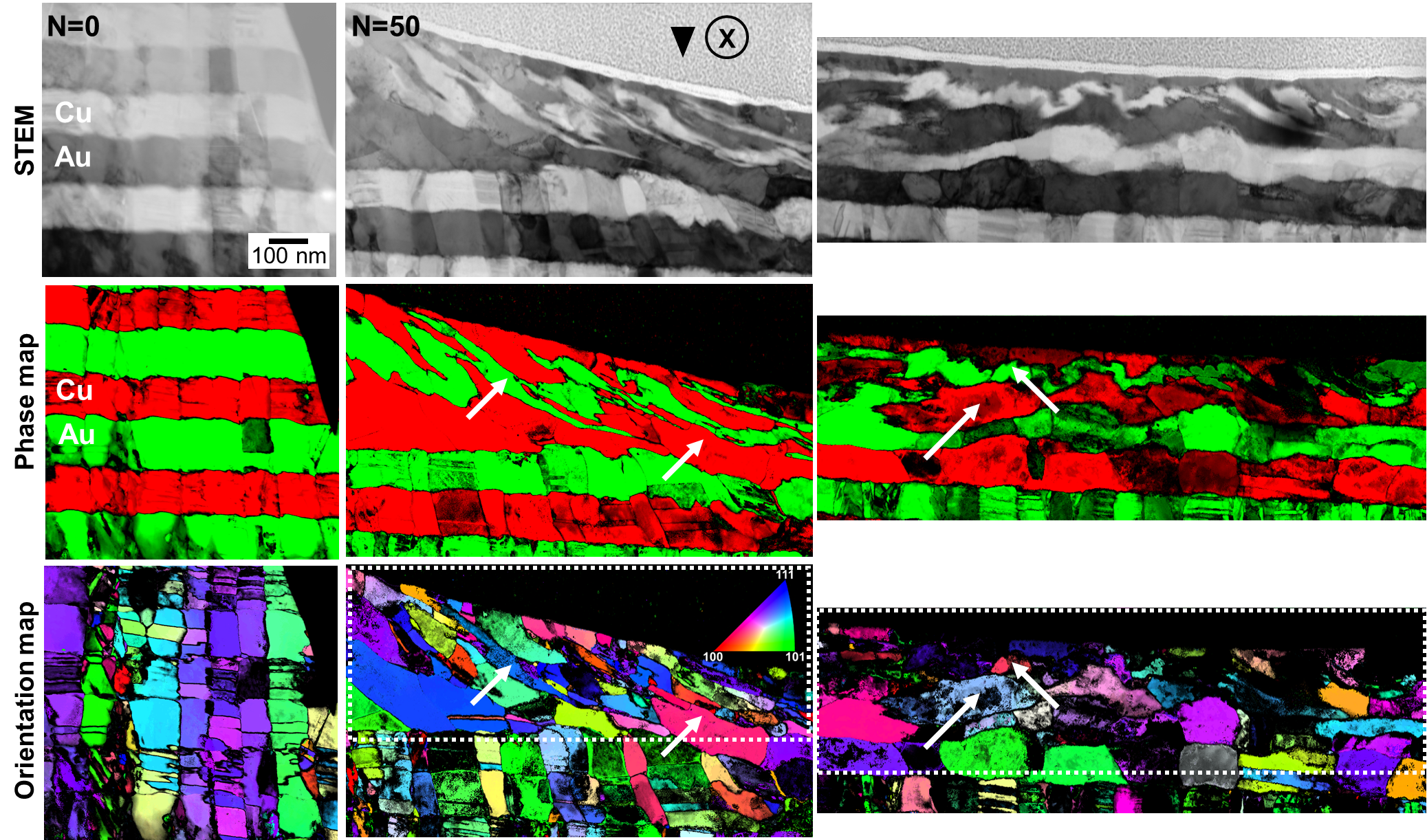
Figure 4.1: ACOM-STEM imaging showing the structure of the Au-Cu multilayers after 50 sliding cycles at 10 mN load showing vortex formation, deformation by detwinning and grain coarsening. White dashed box indicates the deformed region. Vortex formation and mechanical intermixing is also evident in the virtual bright field image.
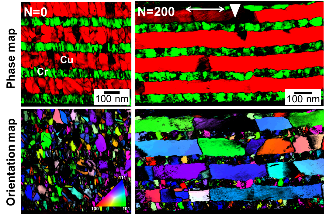
Figure 4.2: ACOM-STEM imaging showing the structure of the Cu-Cr multilayers after 200 sliding cycles at 20 mN load showing grain growth in all the Cu layers.

This project is partially third-party funded by the DAAD PhD scholarship of Ankush Kashiwar.


