Multiscale Modelling
To support accelerating materials development cycles we have developed simulation approaches for de-novo characterization and optimization of materials and device properties with nanoscale constituents. In recent years we have therefore developed simulation methods that describe the conformation and electronic properties of materials built on the basis of well-defined nanoscale constituents, such as single-molecule electronics with application to molecular wires (metallic and organic), development of the atomic transistor, the electronic and structural properties of nanocarbon materials and organic light emitting diodes (OLEDs). In the EU project MMM∂HPC we have developed unified multi-disciplinary approach that integrates materials science simulation and high performance computing is required to transform isolated solutions for specific problems into comprehensive, industry-ready platforms, which are capable of predicting the properties of complex materials on the basis of their constitutive elements.
Currently, we are working on the development of new scale-bridging methods within the Research Training Group (RTG) 2450 - Tailored Scale-Bridging Approaches to Computational Nanoscience. Specifically, our main focus is on the degradation mechanisms in organic electronics and on the DFT-based on-the-fly kinetic Monte Carlo workflow for multiscale modeling of Chemical Vapor Deposition.
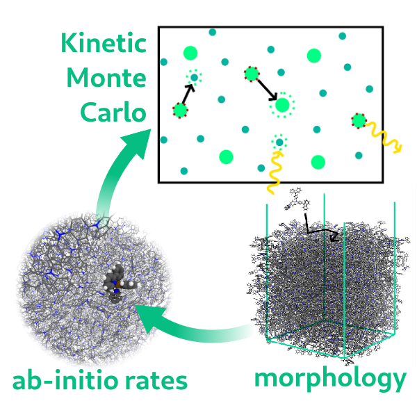
Multiscale Simulation of Photoluminescence Quenching in Phosphorescent OLED Materials
Bimolecular exciton-quenching processes such as triplet–triplet annihilation (TTA) and triplet–polaron quenching play a central role in phosphorescent organic light-emitting diode (PhOLED) device performance and are, therefore, an essential component in computational models. However, the experiments necessary to determine microscopic parameters underlying such processes are complex and the interpretation of their results is not straightforward. Here, a multiscale simulation protocol to treat TTA is presented, in which microscopic parameters are computed with ab initio electronic structure methods. With this protocol, virtual photoluminescence experiments are performed on a prototypical PhOLED emission material consisting of 93 wt% of 4,4ʹ,4ʺ-tris(N-carbazolyl)triphenylamine and 7 wt% of the green phosphorescent dye fac-tris(2-phenylpyridine)iridium. A phenomenological TTA quenching rate of 8.5 × 10⁻¹²cm3s-1, independent of illumination intensity, is obtained. This value is comparable to experimental results in the low-intensity limit but differs from experimental rates at higher intensities. This discrepancy is attributed to the difficulties in accounting for fast bimolecular quenching during exciton generation in the interpretation of experimental data. This protocol may aid in the experimental determination of TTA rates, as well as provide an order-of-magnitude estimate for device models containing materials for which no experimental data are available.
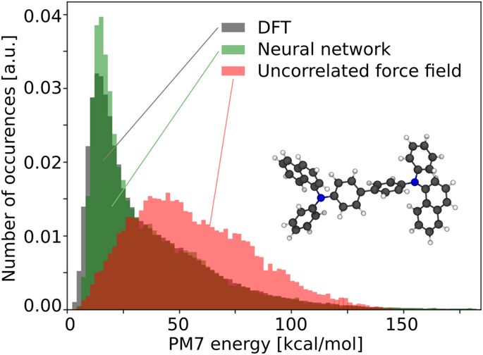
Machine learning of correlated dihedral potentials for atomistic molecular force fields
Molecular mechanics simulations and related computational methods fundamentally rely on the accuracy of classical atomistic force fields for the evaluation of inter- and intramolecular energies. One indispensable component of such force fields, in particular for large organic molecules, is the accuracy of molecule-specific dihedral potentials which are the key determinants of molecular flexibility. Here, we show that non-local correlations of dihedral potentials play a decisive role in the description of the total molecular energy. The latest effect is often neglected in most state-of-the-art dihedral force fields. We, furthermore, report an efficient machine learning approach to compute intramolecular conformational energies on the example of α-NPD. Our approach outperforms traditional force fields by decreasing the mean absolute deviations by one order of magnitude to values smaller than 0.37 kcal/mol (16.0 meV) per dihedral angle.
Rational In Silico Design of an Organic Semiconductor with Improved Electron Mobility
Organic semiconductors find a wide range of applications, such as in organic light emitting diodes, organic solar cells, and organic field effect transistors. One of their most striking disadvantages in comparison to crystalline inorganic semiconductors is their low charge-carrier mobility, which manifests itself in major device constraints such as limited photoactive layer thicknesses. Trial-and-error attempts to increase charge-carrier mobility are impeded by the complex interplay of the molecular and electronic structure of the material with its morphology. Here, the viability of a multiscale simulation approach to rationally design materials with improved electron mobility is demonstrated. Starting from one of the most widely used electron conducting materials (Alq3), novel organic semiconductors with tailored electronic properties are designed for which an improvement of the electron mobility by three orders of magnitude is predicted and experimentally confirmed.
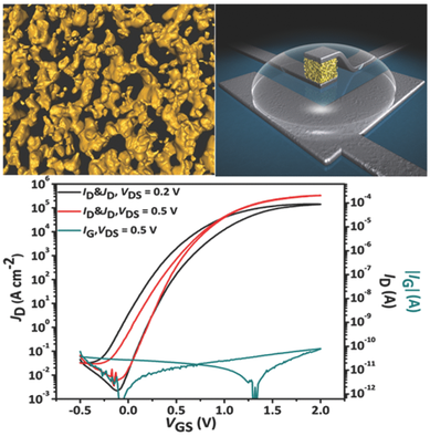
Sub-50 nm Channel Vertical Field-Effect Transistors using Conventional Ink-Jet Printing
A printed vertical field-effect transistor is demonstrated, which decouples critical device dimensions from printing resolution. A printed mesoporous semiconductor layer, sandwiched between vertically stacked drive electrodes, provides <50 nm channel lengths. A polymer-electrolyte-based gate insulator infiltrates the percolating pores of the mesoporous channel to accumulate charge carriers at every semiconductor domain, thereby, resulting in an unprecedented current density of MA cm−2.
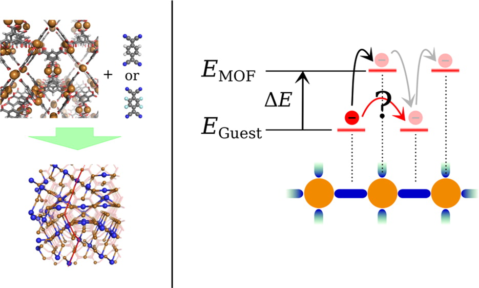
Superexchange Charge Transport in Loaded Metal Organic Frameworks
In the past, nanoporous metal–organic frameworks (MOFs) have been mostly studied for their huge potential with regard to gas storage and separation. More recently, the discovery that the electrical conductivity of a widely studied, highly insulating MOF, HKUST-1, improves dramatically when loaded with guest molecules has triggered a huge interest in the charge carrier transport properties of MOFs. The observed high conductivity, however, is difficult to reconcile with conventional transport mechanisms: neither simple hopping nor band transport models are consistent with the available experimental data. Here, we combine theoretical results and new experimental data to demonstrate that the observed conductivity can be explained by an extended hopping transport model including virtual hops through localized MOF states or molecular superexchange. Predictions of this model agree well with precise conductivity measurements, where experimental artifacts and the influence of defects are largely avoided by using well-defined samples and the Hg-drop junction approach.
Ultrarobust Thin-Film Devices from Self-Assembled Metal–Terpyridine Oligomers
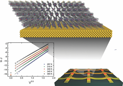
Ultrathin molecular layers of FeII-terpyridine oligomers allow the fabrication of large-area crossbar junctions by conventional electrode vapor deposition. The junctions are electrically stable for over 2.5 years and operate over a wide range of temperatures (150–360 K) and voltages (±3 V) due to the high cohesive energy and packing density of the oligomer layer. Electrical measurements reveal ideal Richardson–Shottky emission in surprising agreement with electrochemical, optical, and photoemission data.
[Au14(PPh3)8(NO3)4], discovery of a new class of Au(NO3)-ligated superatom complexes
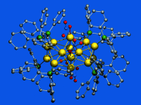
Golden beauty: For the first time a ligand-stabilized Au14 cluster has been examined. The structure of this superatom complex bears several impressive and unique features, which will further support the understanding of certain guiding principles for molecular-precision synthesis and functionalization of ultrasmall nanoparticles.
Angewandte Chemie International Edition 52, 3529–3532 (2013).
Memory effects in electrochemically gated metallic point contacts
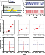
Electrochemical gating permits the observation of few-atom processes in contact reconstruction. We monitor the junction conductance during the opening and closing of an atomic-scale metallic contact and use this as an instantaneous probe of the atomic-scale structural switching process. We observe clear correlations in the quantum conductance of a contact in subsequent switching events, demonstrating memory effects at the atomic scale. These experimental observations are supported by numerical simulations which show a conservation of the contact reconstruction process across several switching cycles. These results open a route to electrochemically control few-atom surface reconstruction events with present-day detection capabilities.
Simulating charge transport in tris(8-hydroxyquinoline) aluminium (Alq3)
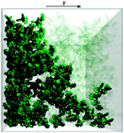
We present a model of charge transport in organic solids which explicitly considers the packing and electronic structure of individual molecules. We simulate the time-of-flight mobility measurement in crystalline and disordered films of tris(8-hydroxyquinoline) aluminium (Alq3). The morphology of disordered Alq3 is modelled on a molecular scale, and density functional theory is used to determine the electronic couplings between molecules. Without any fitting parameters we predict electron mobilities in the crystalline and disordered phases of approximately 1 and approximately 10-4 cm2 V-1 s-1, respectively. In good agreement with experiment we find that electron mobilities are two orders of magnitude greater than those of holes. We explain this difference in terms of the spatial extent of the frontier orbitals. Our results suggest that charge transport in disordered Alq3 is dominated by a few highly conducting pathways.

