
Scanning Probe Microscopy and Nanolithography
Welcome to the website of Prof. Dr. Thomas Schimmel's research unit "Scanning Probe Microscopy and Nanolithography" at the Institute of Nanotechnology at the Karlsruhe Institute of Nanotechnology. We focus on fabrication, analysis, properties and applications of functional nanostructures.
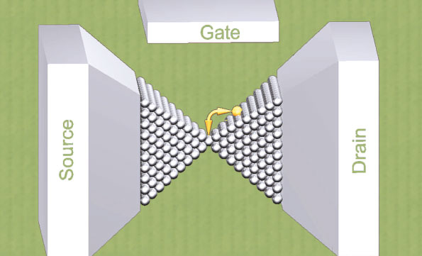
The Atomic Transistor. The controlled repositioning of one single silver atom allows for the reversible opening and closing of an electronic circuit.
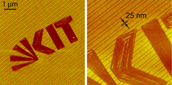
Nanoanalytics and nanolithography via AFM. Functional chemical patterns on surfaces can be written and subsequently imaged with the same AFM tip.
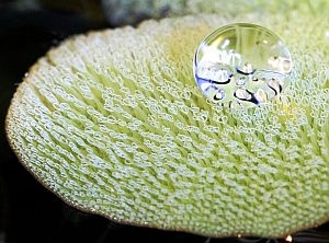
Pattern formation of the nanometer scale by self-organization. An example for biofunctional films is shown.